원자 단위 반도체, 소재별 맞춤형 공정으로 균일하게 만든다
기사입력 2024.05.02 15:07
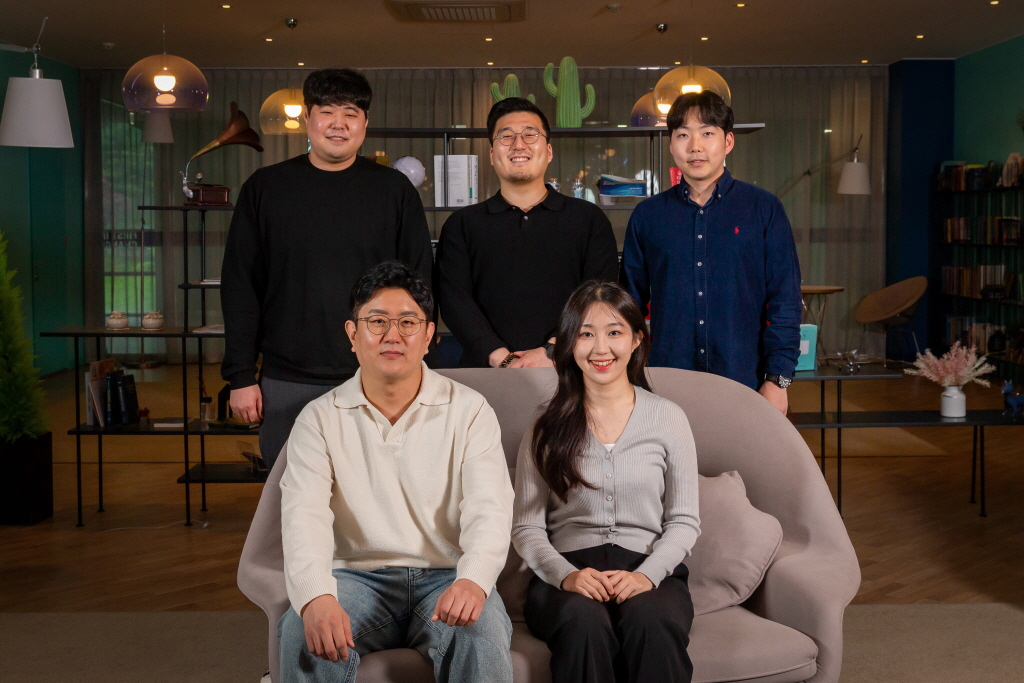
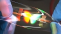
▲이번 연구를 주도한 (윗줄 왼쪽부터)고경민 연구원, 공동 1저자 이욱희 연구원, 조한빈 연구원, (아랫줄 왼쪽부터)서준기 교수, 제 1저자 김성연 연구원
UNIST 서준기 교수팀, 유기금속화학기상증착법 기반 박막 증착 공정법 개발
낮은 온도에서 원자층 두께의 막을 균일하고 안정적으로 입힐 수 있는 공정 기술이 개발됐다.
UNIST(총장 이용훈) 반도체 소재·부품 대학원 및 신소재공학과 서준기 교수팀은 중국과학원 선전선진기술연구원 Feng Ding 교수, 세종대학교 김성규 교수, UNIST 정창욱 교수팀과 함께 유기금속화학기상증착법(Metal-organic chemical vapor deposition, MOCVD)을 활용해 200도의 저온에서 주석 셀라나이드계 소재별 맞춤형 공정법으로 얇은 막을 웨이퍼 단위의 대면적에 증착시킬 수 있는 박막 증착 공정법을 개발했다고 2일 밝혔다.
유기금속화학기살증착법은 화학반응에 참여하는 기체상의 전구체를 활용해 우수한 정밀성을 가지는 차세대 공정법이다. 반도체의 재료가 되는 웨이퍼 정도의 큰 면적에도 박막을 증착시킬 수 있다. 하지만 반응물을 합성시키기 위해선 650도 이상의 높은 온도로 리간드를 분해해야 했다.
연구팀은 전자소자, 광학소자, 열전소자 등 다양한 분야에서 연구 중인 2종의 주석 셀레나이드계 물질(SnSe2, SnSe)에 유기금속화학기상증착법을 적용했다. 2종의 주석 셀레나이드 박막 모두 웨이퍼 단위의 수 나노 수준 두께로 균일하게 증착시켰다.
연구팀은 낮은 온도로 증착하기 위해 리간드가 분해되는 온도 구간과 박막이 증착되는 온도 구간을 물리적으로 분리했다. 증착법에 사용되는 주석과 셀레늄 전구체의 비율을 조절하고, 전구체를 운반하는 알곤가스의 유량도 정밀히 조절했다.
이렇게 제조된 박막은 높은 결정성을 갖는다. 규칙적으로 배열되는 것이다. 증착 과정에서 물질의 상(phase)과 두께도 제어할 수 있다. 유기금속화학기상증착법을 사용했음에도 200도 정도의 저온에서 기판 종류와 상관없이 균일하게 증착됐다.
연구팀은 개발된 공정을 웨이퍼 전체에 적용했다. 2종의 박막 모두 화학적으로 변하지 않고 높은 결정성을 가졌다. 원자층 수준의 두께 조절과 균일한 증착도 가능했다. 개발된 공정법이 다양한 전자소자에 대면적으로 활용될 수 있음을 보여주는 것이다.
제 1저자 김성연 연구원은 “이번 연구는 기존 유기금속화학기상증착법의 한계를 극복하고 다상계의 물질을 화학적 조성이 변하지 않으면서 대면적으로 증착할 수 있었다”며 “향후 주석 셀레나이드계 박막의 소재연구 뿐 아니라 다양한 전자소자에 응용이 가능할 것이다”고 전했다.
서준기 교수는 “이번 연구는 반도체 박막 소재 상(Phase)에 따른 고유의 열역학과 동력학적 거동 기반 공정 전략을 제시한 사례이다”며 “차세대 반도체 소재 맞춤형 공정 개발에 성공했다는 점에서 전자소자 응용 연구를 가속화 시킬 것”이라고 전했다.
이번 연구는 나노과학 분야 국제 학술지 ‘Advanced Materials’에 4월10일 온라인 게재됐다. 연구 수행은 과학기술정보통신부 한국연구재단 우수신진연구사업 및 차세대지능형반도체기술개발(소자)사업, 울산과학기술원 등의 지원으로 수행됐다.
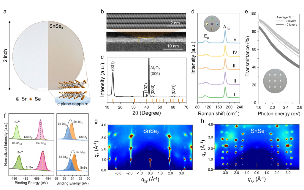
▲증착된 2종의 셀렌화 주석박막의 웨이퍼 단위 대면적 성장 및 성장된 박막의 결정성 및 상·두께 균일도 분석

관련뉴스
-

친환경 유기 배터리 수명, 새로운 전해질로 향상
UNIST(총장 이용훈) 에너지화학공학과 곽원진 교수팀이 한양대 기계공학과 최준명 교수팀과 공동으로 유기 전극의 장점을 유지하면서 획기적으로 전지의 성능을 향상시킬 수 있는 전해질을 개발했다.
2024-02-01 오후 4:22:09by 배종인 기자
-
UNIST, 현대차와 차세대 3D 프린팅 맞손
UNIST(총장 이용훈)는 현대자동차(대표이사 이동석)와 울산시 남구 두왕동 UNIST 산학융합캠퍼스 내 3D프린팅 융합기술센터에서 ‘3D프린팅 공동 연구개발실 운영을 위한 상호 협력 약정’을 체결했다.
2024-02-05 오후 3:01:39by 배종인 기자
-

UNIST, 기존 재료 한계 뛰어넘는 기계적 메타 물질 개발
UNIST(총장 이용훈) 신소재공학과 김지윤 교수팀이 기존의 재료의 한계를 뛰어넘어 실시간으로 물질의 모양과 특성을 조절할 수 있는 메타 물질을 세계 최초로 개발했다.
2024-02-05 오후 3:05:29by 배종인 기자
-
수소 경제성, 저장 밀도 높여 달성
UNIST(총장 이용훈) 화학과 오현철 교수는 보통의 대기압에서도 수소를 고밀도로 저장할 수 있는 나노다공성 수소화붕소마그네슘 구조(Mg(BH4)2)를 보고했다.
2024-02-13 오후 2:14:28by 배종인 기자
-

UNIST, 산화력 뛰어난 금속-플루오린 촉매 개발
UNIST(총장 이용훈) 화학과 조재흥 교수팀이 산화력이 뛰어난 새로운 망간-플루오린 촉매 합성에 성공했다.
2024-02-21 오전 11:50:00by 배종인 기자
-
고무처럼 늘려도 화질변화 없는 디스플레이 나왔다
기초과학연구원(IBS, 원장 노도영) 나노입자 연구단 김대형 부연구단장(서울대 화학생물공학부 교수)과 현택환 단장(서울대 화학생물공학부 석좌교수) 연구팀은 최문기 UNIST 교수, 양지웅 DGIST 교수팀과 공동으로 세계 최고 성능의 스트레처블 QLED(퀀텀닷발광다이오드) 개발에 성공했다.
2024-04-16 오전 9:44:12by 배종인 기자
-
.jpg)
태양에너지만으로 고효율 암모니아 생산
UNIST(총장 이용훈) 에너지화학공학과 장지욱, 장성연 교수팀은 스탠퍼드 대학교 Thomas F. Jaramillo 교수와 공동으로 페로브스카이트 기반 친환경 암모니아 생산 광전극 시스템을 개발했다. 이 기술을 이용하면 태양에너지만으로 고효율의 암모니아를 생산할 수 있을 것으로 기대된다.
2024-04-16 오후 4:03:06by 배종인 기자

.png)
관련 웨비나


많이 본 뉴스
[열린보도원칙] 당 매체는 독자와 취재원 등 뉴스이용자의 권리 보장을 위해 반론이나 정정보도, 추후보도를 요청할 수 있는 창구를 열어두고 있음을 알려드립니다.
고충처리인 장은성 070-4699-5321 , news@e4ds.com