국내외 AI 반도체 및 데이터센터 등 AI 시장 핵심 인프라에 대한 투자가 촉진되고 있다. 삼성전자는 2021년 메모리 반도체와 AI 프로세서를 하나로 결합한 ‘HBM-PIM’을 지속 발전시키고 있다. SK하이닉스는 AI 추론·학습 성능에 최적화된 차세대 적층형 메모리 ‘HBM3’ 개발에 성공했다. 데이터센터는 빅데이터를 수집·저장·분석할 수 있는 클라우드 컴퓨팅 서비스를 제공하며, AI 모델을 훈련하는 데 적합하다. 국내에서 AI 반도체 개발과 함께 안정적인 인프라 확보를 위한 데이터센터 투자가 가속화되고 있다.
▲작년 10월 ‘삼성 테크 데이 2022’ 메모리사업부장 이정배 사장
챗GPT, 특화된 고성능·고용량 AI 반도체 뒷받침 必
삼성전자 ‘HBM-PIM’, 메모리 반도체 연산기능 탑재
데이터센터 시장 급부상…AI 성능↑·안정적인 데이터 처리
챗GPT 열풍이 불며 온갖 헤드라인을 장식하고 있다. 초거대 AI 모델은 인간처럼 대규모 학습 및 빠른 연산을 할 수 있는 AI로, 이를 구현하기 위해서는 전용 반도체와 이를 수행할 수 있는 컴퓨팅 인프라를 필요로 한다. 이에 따라 국내외 AI 반도체 및 데이터센터 등 AI 시장 핵심 인프라에 대한 투자가 촉진되고 있다.
AI 시대에서 중요한 점은 고성능 프로세서 구동을 위해서는 고성능·고용량의 메모리가 필수적이라는 것이다. GPU 또는 AI 가속기에 직접 데이터를 제공하는 고대역폭 메모리(HBM, High Bandwidth Memory)를 비롯해 128GB 이상의 고용량 서버 D램의 수요가 모두 증가할 것으로 예측된다.
특히 한국이 시장 주도권을 잡기 위해 강세를 점하고 있는 메모리 분야를 기반으로, 대량 연산이 가능한 고성능 프로세스와 이를 지원하는 고용량 메모리 조합이 각광받고 있다. 장기적으로 메모리에 특화된 AI 반도체가 생성 AI의 성능을 좌우할 것이라는 전망이 잇따라 나오고 있다.
■ 삼성전자-꽉 쥐고있는 ‘PIM’, SK하이닉스-꾸준한 메모리 혁신
삼성전자는 2021년 메모리 반도체와 AI 프로세서를 하나로 결합한 ‘HBM-PIM’을 지속 발전시키고 있다.
삼성전자는 지난 1월 2022년 실적 컨퍼런스콜에서 “자연어 기반 대화형 AI 서비스가 차세대 메모리 수요에 영향을 끼칠 것”이라 말했다.
‘PIM(Processing-in-memory)’은 메모리 내부에 연산 작업을 하는 AI 프로세서 기능을 더한 메모리다. 메모리 간 다량의 데이터 이동을 줄여 AI 가속기 시스템의 성능과 효율을 높였다.
여기서 나온 HBM-PIM은 AI 가속기의 성능을 극대화하는 AI 맞춤형 솔루션으로 급부상했다. HBM은 고성능 컴퓨터(HPC)의 고속 처리를 향상시키는 역할을 담당해왔다. HBM은 D램의 한계를 보완할 수 있는 차세대 메모리로 수요가 증가할 것으로 예상되고 있다. AMD는 삼성전자와 협력을 통해 AI 프로세서 ‘MI-100’에 삼성전자의 HBM-PIM 메모리를 탑재한 바 있다.
PIM인공지능반도체 심포지움에서 삼성전자 손교민 마스터는 “AI 시스템에 HBM-PIM을 탑재할 경우 기존 HBM2를 이용한 시스템 대비 성능은 약 2배 이상 높아지고, 시스템 에너지는 70% 이상 감소된다”고 말했다.
한편 삼성전자는 작년 12월 네이버와 손을 잡았다. 양사는 AI 시스템 병목 해결 및 전력 효율 극대화를 위해 협력키로 했다. 삼성전자의 반도체 설계·제조 기술에 네이버의 AI 알고리즘 개발·검증, AI 서비스 경험을 융합해 차세대 AI 전용 반도체 솔루션을 개발한다.
네이버클라우드 곽용재 CTO는 “삼성전자와 함께 LLM(대규모언어모델)의 연산·학습·추론에 필요한 기능을 모두 갖추면서, 기존 GPU의 1/10 크기의 모델 사이즈, 4배 이상의 전력 효율성을 갖춘 경량화 된 AI 반도체 솔루션을 만들고 있다"고 설명했다.
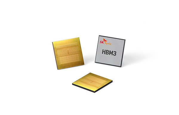
▲SK하이닉스 HBM3
SK하이닉스는 AMD와 함께 세계 최초의 HBM 제품을 개발하는 등 HBM 분야에서 오랜 역량을 갖춰왔다. 작년 10월에는 AI 추론·학습 성능에 최적화된 차세대 적층형 메모리 ‘HBM3’ 개발에 성공했다.
HBM3는 16Gb 코어 다이 밀도와 TSV(Through Silicon Via) 기술의 조합으로 더 높은 집적도의 시스템 레벨의 요구 수준을 충족시켰다. 엔비디아 H100에 결합해 기존 HBM2E보다 데이터 처리 속도는 78% 향상된 것으로 나타났다.
지난 1월에는 모바일용 D램 ‘LPDDR5T’를 개발하며 꾸준히 기술 리더십을 발휘하고 있다. LPDDR5X 대비 13% 빨라진 초당 9.6기가비트의 초고속을 자랑하는 해당 제품은 전압 기준 1.01~1.12V에서 작동해 초저전력 특성도 구현해냈다. 이는 10나노급 4세대(1a) 미세공정 기반으로 하반기에 양산이 돌입된다.
SK하이닉스는 “이번 LPDDR5T의 활용 범위가 스마트폰뿐 아니라 AI, 머신러닝, AR/VR로 확대될 것으로 기대하고 있다”고 말했다.
메모리 반도체 이외 이통 3사와 손잡은 사피온, 리벨리온, 퓨리오사AI 등도 국산 AI 반도체 기업들도 출사표를 던지고 있다. 메타, 네이버, 카카오 등도 대규모 언어 모델을 출시할 계획을 발표하며 경쟁에서 빠지지 않고 있다.
■ AI 구현 필수 인프라, 데이터센터 투자 확대
수십억 개의 매개변수를 갖는 AI 모델의 대규모 연산을 위해 AI 반도체뿐만 아니라 AI 성능을 높이고 데이터 처리를 안정적으로 뒷받침하기 위한 데이터센터의 역할이 중요해졌다.
데이터센터는 빅데이터를 수집·저장·분석할 수 있는 클라우드 컴퓨팅 서비스를 제공하며, AI 모델을 훈련하는 데 적합하다. 국내에서 AI 반도체 개발과 함께 안정적인 인프라 확보를 위한 데이터센터 투자가 가속화되고 있다.
.jpg) ▲데이터센터
▲데이터센터 ‘각 세종’ 설립 목표를 전한 네이버
네이버클라우드는 춘천 데이터센터 운영 역량을 기반으로 ‘각 세종’ 설립에 나서고 있다. '각 세종'은 올해 2분기 내 준공을 완료하고 3분기에 실가동을 목표로 한다. '각 세종'은 AI 인프라를 효율성 증대를 위해 안정적인 전원 용량을 확보하고, 냉방 기술을 갖춘다.
네이버클라우드 정수환 IT서비스본부장은 “각 세종은 최근 주목받고 있는 네이버의 초대규모 AI 하이퍼클로바가 성장하고 전세계로 뻗어나가는 근간이 될 것”이라고 말했다.
곽용재 네이버클라우드 최고기술책임자(CTO)는 "초대규모 AI가 향후 더욱 고도화될 것임을 고려할 때, 소프트웨어-하드웨어-운영 환경에 대한 통합적 접근이 필요하다"며, “삼성전자와 협력해 개발하는 AI 반도체 솔루션을 각 세종에서 운영할 경우 더 효율적이고 안정적인 운영이 가능하다”고 덧붙였다.
SKT는 자사의 AI 서비스 ‘에이닷’의 성장에 따라 데이터센터 사업의 운영 효율화에 나섰다.
SKT는 지난 2월 자사의 초거대 AI 모델인 ‘에이닷’의 두뇌인 슈퍼컴퓨터 ‘타이탄’을 기존 대비 2배인 NVIDIA A100 GPU를 1040개로 확대 구축했다. 이로써 SKT의 슈퍼컴퓨터는 17.1 페타플롭 이상의 성능을 지원해 에이닷은 기존보다 저 정교한 학습을 할 수 있게 됐다.
■ AI 반도체 부상과 함께 DPU 성장 주목
이러한 흐름에서 DPU(Data Processing Unit)는 주목할 만한 키워드다. DPU는 고성능 서버에 탑재된 CPU·GPU 등의 데이터 처리를 담당하는 프로세서로, 더 빠르고 확장 가능한 데이터센터를 지원한다.
마켓앤마켓에 따르면, 글로벌 DPU 시장은 연평균 약 35%씩 성장해 2027년까지 약 100조원 규모로 성장할 것으로 전망된다.
젠슨 황(Jensen Huang) 엔비디아 창립자 겸 CEO의 말을 인용하면, “CPU와 GPU에 이어, DPU는 데이터 중심 가속 컴퓨팅의 또 하나의 핵심 축이 될 것”이며, “CPU는 범용 컴퓨팅, GPU는 가속 컴퓨팅을 위한 것이라면, 데이터센터에서 데이터를 이동시키는 DPU는 데이터 처리를 담당할 것"이다.
 ▲
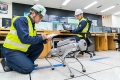
▲이종호 과기부 장관이 2일 망고부스트를 방문해 김장우 망고부스트 대표로부터 DPU에 대한 설명을 듣고 있다.
지난 2월 28일 과기부는 이종호 장관, DPU 스타트업 ㈜망고부스트를 방문해 개발현황과 성과를 공유했다.
망고부스트는 서울대학교 전기정보공학부 김장우 교수가 제자들과 함께 올해 설립한 스타트업으로, DPU 관련 반도체 및 소프트웨어 개발 전문 업체다. 작년 130억원 규모 투자를 유치한 바 있다. 망고부스트는 “DPU는 애플리케이션 성능을 크게 향상시키고 인프라 처리를 위한 CPU 및 서버 비용을 줄인다”고 주장한다.
과기부는 “챗GPT 등 초거대 AI 개발 경쟁이 치열해지고 있는 가운데, 초거대 AI의 기반이 되는 데이터센터에서 사용되는 DPU 역시 그 시장의 급속 성장이 예상된다”며, “현재 집중 지원되고 있는 AI 반도체와 더불어 데이터처리 관련 반도체 기술의 개발이 중요해지고 있다”고 말했다.
.jpg)
.JPG)


.JPG)