기사입력 2024.02.13 12:45
인텔이 연례 개발자 행사인 세번째 인텔 이노베이션(Intel Innovation)을 美 캘리포니아주 산호세에서 개최하며, 클라이언트, 엣지, 네트워크 및 클라우드에 이르는 모든 워크로드에서 인공지능 접근성을 높이고 사용할 수 있도록 지원하는 다양한 기술을 공개했다.
2023-09-20 오전 11:44:25by 배종인 기자

반도체 및 첨단 웨이퍼 레벨 패키징(WLP) 애플리케이션을 위한 웨이퍼 처리 솔루션 전문 기업인 ACM 리서치(ACM Research)가 새로운 진공 세정 솔루션을 발표하며, 첨단 3D 패키지의 새로운 세정 요구 사항을 충족 시켰다.
2023-09-27 오전 10:32:33by 배종인 기자
이종호 과학기술정보통신부 장관이 LG이노텍에서 반도체 첨단 패키징용 기판에 관한 연구 현장을 살펴보고 산학연 전문가들이 참여하는 간담회 개최를 통해 반도체 첨단 패키징 관련 연구개발(R&D) 사업에 대한 의견을 청취했다.
2023-12-05 오전 10:29:09by 배종인 기자
갑진년 새해에는 반도체, 디스플레이, 이차전지 3대 주력기술 분야에서 차세대 원천기술 확보를 위한 지원이 가속화될 전망이다.
2024-01-02 오전 9:07:52by 권신혁 기자

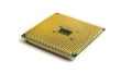
인텔이 최첨단 3D 패키징 기술의 대량 생산이 가능한 최첨단 반도체 생산시설 ‘팹 9(Fab 9)’을 오픈했다.
2024-01-25 오후 3:30:38by 배종인 기자

MEMS, 나노기술, 반도체 시장용 웨이퍼 본딩 및 리소그래피 장비 분야를 선도하는 EV Group이 적외선(IR) 레이저를 적용한 EVG의 레이어 분리 신기술을 통해 첨단 패키징에서 트랜지스터 소형화까지 박막 3D 적층을 실현했다.
2024-02-01 오후 3:18:03by 배종인 기자

[열린보도원칙] 당 매체는 독자와 취재원 등 뉴스이용자의 권리 보장을 위해 반론이나 정정보도, 추후보도를 요청할 수 있는 창구를 열어두고 있음을 알려드립니다.
고충처리인 장은성 070-4699-5321 , news@e4ds.com